
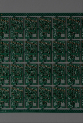
Double Sided PCBs
Double Sided PCBs
Certificates:ISO-certified
Savli, GJ
Storefront →Price on request
MOQ — Lead time on requestCurrency INR
BharatSeal order protection
Secure payments
Every payment is processed via Razorpay with PCI-DSS data protection and SSL encryption. We never see your card details.
PayUPIVisaMCAmexRuPayNet BankingWalletsPay Later+ more
Money-back protection
Claim a refund if your order doesn't ship, arrives damaged, or doesn't match the agreed spec. Disputes resolved within 7 working days.
Trade Assurance — not yet enrolled by this seller
This seller has not yet activated Trade Assurance. Pay outside BharatSeal at your own risk — we recommend chatting first to verify.
Only orders placed and paid through BharatSeal can enjoy free protection by 🛡 BharatSeal Trade Assurance.
Highlights at a glance
- ✓Category: Double Sided PCBs
- ✓Made in Savli, GJ, India
- ✓Certified: ISO-certified
About this item
- Higher Packaging Density: It enables designers to reduce the physical size of their circuit board assemblies by packing components more closely together, thus improving their overall design efficiency.
- Cost Reduction: Double sides PCBs save cost to some extent as it reduces the number of boards required for a given circuit design, and hence cost per unit is reduced.
- Improved Performance: Double-sided PCBs have better performance due to higher interconnectivity, which improves the signal integrity of the board and also reduces noise interference from external sources.
- Greater Flexibility: Designers can create complex circuits as double-sided PCBs allow for more routing options than single-sided boards, thus providing greater flexibility in design.
- Increased Reliability: Double-sided PCBs are more reliable than single-sided ones due to the increased number of electrical connections and insulation layers, which helps prevent short circuits and reduces errors.
Description
A double-sided printed circuit board (PCBs) is a type of printed circuit board that has two sides with conductive layers and components connected via plated holes.
This type of PCBs is used in many applications, such as computers, automotive electronics, medical devices, telecommunication systems and consumer electronics. They allow for increased density and better electrical performance, making them the preferred choice for more complex designs.
Due to their double layer of conductive material, they tend to be slightly more expensive than single-sided PCBs, but their improved performance makes them an investment worth making for larger projects. Whether a hobbyist or a professional manufacturer, double-sided printed circuit boards are the perfect choice for more extensive projects needing reliable performance.
Double-Sided PCBs Manufacturing Process:
- **Step 1: Design and Output**
The first step in double-sided PCBs manufacturing is the design of the printed circuit board. The output will be a Gerber file containing detailed information about what components need to be included, where they should go, and any other necessary specifications. The manufacturer will use this file to create the boards.
- **Step 2: From File to Film**
Once the design is complete, the manufacturer will then use a special machine or software to create films that contain all of the necessary information to produce the board. This includes things such as tracks, pads, and drill holes.
- **Step 3: Printing the Inner layers: Where Will the Copper Go?**
The film from step 2 will be used to create the inner layers of the board. This is done using a machine that prints electrically conductive ink onto a substrate. The printed circuit board layers then have copper sheets bonded to them to complete each layer.
- **Step 4: Removing the Unwanted Copper**
Once the inner layers are complete, any unwanted copper is then removed. This process is known as ‘etching’, and it involves using a chemical solution in order to dissolve away the unwanted copper from each layer.
- **Step 5: Layer Alignment and Optical Inspection**
After the etching process is complete, the layers are then aligned to ensure that each layer is correctly placed. The alignment process is done using optical inspection, which allows for a precise alignment check between all layers.
- **Step 6: Layer-up and Bond**
Once the layers have been aligned, they are then bonded together in order to create one single board. This is done using a unique adhesive that is applied between each layer.
- **Step 7: Drill**
The next step involves drilling holes in the board to make room for components such as resistors and capacitors. This is done using a machine that drills through each layer simultaneously, meaning that all holes are perfectly placed on each layer.
- **Step 8: Plating and Copper Deposition** Once the drilling is complete, a plating process is then used to deposit copper onto the inner and outer surfaces of the board. This creates a conductive layer that can be used for tracks and pads.
- **Step 9: Outer Layer Imaging** The image from Step 2 will then be applied to the outer layer of the board, in order to create the tracks, pads and other features that were specified in the design. This is done using a machine that applies a special ink or film onto each layer.
- **Step 10: Plating**
Once the outer layers have been imaged, a plating process is then used to deposit copper onto the board’s surface. This plating process is used in order to create tracks and pads, which can then be connected to components.
- **Step 11: Final Etching**
Once the plating and imaging processes are complete, any unwanted copper is removed from the board’s surface using a chemical etching process. This etching process removes any unnecessary copper which could otherwise cause short circuits or other electrical issues.
- **Step 12: Solder Mask Application** A solder mask is then applied to the board to protect it from any corrosion and reduce any potential contact between components that could result in short circuits. The solder mask is a special coating applied to the board’s surface, and it helps prevent damage.
- **Step 13: Final Inspection** The final step in the PCBs manufacturing process is a thorough board inspection. This is done to ensure that all components are correctly placed, that any shorts or opens have been identified and corrected, and that the tracks and pads are connected correctly. Once the board has passed this final inspection, it is then ready for use!
Benefits of Double-Sided PCBs India:
- Higher Packaging Density: It enables designers to reduce the physical size of their circuit board assemblies by packing components more closely together, thus improving their overall design efficiency.
- Cost Reduction: Double sides PCBs save cost to some extent as it reduces the number of boards required for a given circuit design, and hence cost per unit is reduced.
- Improved Performance: Double-sided PCBs have better performance due to higher interconnectivity, which improves the signal integrity of the board and also reduces noise interference from external sources.
- Greater Flexibility: Designers can create complex circuits as double-sided PCBs allow for more routing options than single-sided boards, thus providing greater flexibility in design.
- Increased Reliability: Double-sided PCBs are more reliable than single-sided ones due to the increased number of electrical connections and insulation layers, which helps prevent short circuits and reduces errors.
What are the Applications of Double-Sided PCBs?
- Computer and Telecommunications: Double-sided PCBs are widely used in computers, portable devices, networking equipment, and telecommunications systems to reduce the size of their assemblies.
- Automotive: Double-sided PCBs are often used in automotive applications due to their improved signal integrity and reduced size. Examples include electronic control units (ECUs), engine management, and airbag systems.
- Consumer Electronics: Double-sided PCBs are also used in a range of consumer electronics such as TVs, DVD players, mobile phones, audio equipment, and gaming consoles.
- Medical Instruments: Apart from being used in medical diagnostic and therapeutic devices, double-sided PCBs are also used in medical instruments to provide greater reliability and accuracy.
- Military Equipment: Double-sided PCBs are frequently used in military equipment, such as missiles, aircraft and spacecraft, radar systems, and navigation systems due to their superior performance.
- Industrial Control: Industrial control systems also benefit from double-sided PCBs due to the improved signal integrity they provide and greater reliability. Examples include robotics, machine vision systems and power distribution systems.
Key attributes
Certificates
ISO-certified
Reviews
Questions & answers
Ask the supplier — answers are visible to all buyers
No questions yet. Be the first to ask!
Know your supplier
MEENA CIRCUITS PRIVATE LIMITED
Unverified<1 yr on BharatSealSavli, Gujarat
Orders completed
—
On-time delivery
—
Reorder rate
—
Year founded
2006
Staff size
—
Certifications
1


%22%2F%3E%3Ctext%20x%3D%2250%25%22%20y%3D%2250%25%22%20dominant-baseline%3D%22central%22%20text-anchor%3D%22middle%22%20font-family%3D%22'DM%20Sans'%2Csystem-ui%2Csans-serif%22%20font-weight%3D%22800%22%20font-size%3D%22126%22%20fill%3D%22%231a1a1a%22%20fill-opacity%3D%220.14%22%20letter-spacing%3D%22-2%22%3ESS%3C%2Ftext%3E%3C%2Fsvg%3E)
%22%2F%3E%3Ctext%20x%3D%2250%25%22%20y%3D%2250%25%22%20dominant-baseline%3D%22central%22%20text-anchor%3D%22middle%22%20font-family%3D%22'DM%20Sans'%2Csystem-ui%2Csans-serif%22%20font-weight%3D%22800%22%20font-size%3D%22126%22%20fill%3D%22%231a1a1a%22%20fill-opacity%3D%220.14%22%20letter-spacing%3D%22-2%22%3ESS%3C%2Ftext%3E%3C%2Fsvg%3E)
%22%2F%3E%3Ctext%20x%3D%2250%25%22%20y%3D%2250%25%22%20dominant-baseline%3D%22central%22%20text-anchor%3D%22middle%22%20font-family%3D%22'DM%20Sans'%2Csystem-ui%2Csans-serif%22%20font-weight%3D%22800%22%20font-size%3D%22126%22%20fill%3D%22%231a1a1a%22%20fill-opacity%3D%220.14%22%20letter-spacing%3D%22-2%22%3EDS%3C%2Ftext%3E%3C%2Fsvg%3E)
%22%2F%3E%3Ctext%20x%3D%2250%25%22%20y%3D%2250%25%22%20dominant-baseline%3D%22central%22%20text-anchor%3D%22middle%22%20font-family%3D%22'DM%20Sans'%2Csystem-ui%2Csans-serif%22%20font-weight%3D%22800%22%20font-size%3D%22126%22%20fill%3D%22%231a1a1a%22%20fill-opacity%3D%220.14%22%20letter-spacing%3D%22-2%22%3EDS%3C%2Ftext%3E%3C%2Fsvg%3E)
%22%2F%3E%3Ctext%20x%3D%2250%25%22%20y%3D%2250%25%22%20dominant-baseline%3D%22central%22%20text-anchor%3D%22middle%22%20font-family%3D%22'DM%20Sans'%2Csystem-ui%2Csans-serif%22%20font-weight%3D%22800%22%20font-size%3D%22126%22%20fill%3D%22%231a1a1a%22%20fill-opacity%3D%220.14%22%20letter-spacing%3D%22-2%22%3EDS%3C%2Ftext%3E%3C%2Fsvg%3E)
%22%2F%3E%3Ctext%20x%3D%2250%25%22%20y%3D%2250%25%22%20dominant-baseline%3D%22central%22%20text-anchor%3D%22middle%22%20font-family%3D%22'DM%20Sans'%2Csystem-ui%2Csans-serif%22%20font-weight%3D%22800%22%20font-size%3D%22126%22%20fill%3D%22%231a1a1a%22%20fill-opacity%3D%220.14%22%20letter-spacing%3D%22-2%22%3EDS%3C%2Ftext%3E%3C%2Fsvg%3E)
%22%2F%3E%3Ctext%20x%3D%2250%25%22%20y%3D%2250%25%22%20dominant-baseline%3D%22central%22%20text-anchor%3D%22middle%22%20font-family%3D%22'DM%20Sans'%2Csystem-ui%2Csans-serif%22%20font-weight%3D%22800%22%20font-size%3D%22126%22%20fill%3D%22%231a1a1a%22%20fill-opacity%3D%220.14%22%20letter-spacing%3D%22-2%22%3EDS%3C%2Ftext%3E%3C%2Fsvg%3E)
%22%2F%3E%3Ctext%20x%3D%2250%25%22%20y%3D%2250%25%22%20dominant-baseline%3D%22central%22%20text-anchor%3D%22middle%22%20font-family%3D%22'DM%20Sans'%2Csystem-ui%2Csans-serif%22%20font-weight%3D%22800%22%20font-size%3D%22126%22%20fill%3D%22%231a1a1a%22%20fill-opacity%3D%220.14%22%20letter-spacing%3D%22-2%22%3EDS%3C%2Ftext%3E%3C%2Fsvg%3E)
%22%2F%3E%3Ctext%20x%3D%2250%25%22%20y%3D%2250%25%22%20dominant-baseline%3D%22central%22%20text-anchor%3D%22middle%22%20font-family%3D%22'DM%20Sans'%2Csystem-ui%2Csans-serif%22%20font-weight%3D%22800%22%20font-size%3D%22126%22%20fill%3D%22%231a1a1a%22%20fill-opacity%3D%220.14%22%20letter-spacing%3D%22-2%22%3EDS%3C%2Ftext%3E%3C%2Fsvg%3E)
%22%2F%3E%3Ctext%20x%3D%2250%25%22%20y%3D%2250%25%22%20dominant-baseline%3D%22central%22%20text-anchor%3D%22middle%22%20font-family%3D%22'DM%20Sans'%2Csystem-ui%2Csans-serif%22%20font-weight%3D%22800%22%20font-size%3D%22126%22%20fill%3D%22%231a1a1a%22%20fill-opacity%3D%220.14%22%20letter-spacing%3D%22-2%22%3EDS%3C%2Ftext%3E%3C%2Fsvg%3E)
%22%2F%3E%3Ctext%20x%3D%2250%25%22%20y%3D%2250%25%22%20dominant-baseline%3D%22central%22%20text-anchor%3D%22middle%22%20font-family%3D%22'DM%20Sans'%2Csystem-ui%2Csans-serif%22%20font-weight%3D%22800%22%20font-size%3D%22126%22%20fill%3D%22%231a1a1a%22%20fill-opacity%3D%220.14%22%20letter-spacing%3D%22-2%22%3EDS%3C%2Ftext%3E%3C%2Fsvg%3E)