Stencils
Certificates:ISO 9001:2015
Bangalore, KA
Storefront →Price on request
MOQ — Lead time on requestCurrency INR
BharatSeal order protection
Secure payments
Every payment is processed via Razorpay with PCI-DSS data protection and SSL encryption. We never see your card details.
PayUPIVisaMCAmexRuPayNet BankingWalletsPay Later+ more
Money-back protection
Claim a refund if your order doesn't ship, arrives damaged, or doesn't match the agreed spec. Disputes resolved within 7 working days.
Trade Assurance — not yet enrolled by this seller
This seller has not yet activated Trade Assurance. Pay outside BharatSeal at your own risk — we recommend chatting first to verify.
Only orders placed and paid through BharatSeal can enjoy free protection by 🛡 BharatSeal Trade Assurance.
Highlights at a glance
- ✓Made in Bangalore, KA, India
- ✓Certified: ISO 9001:2015
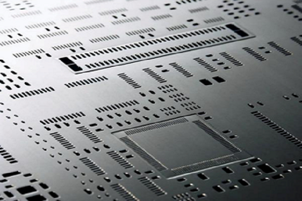
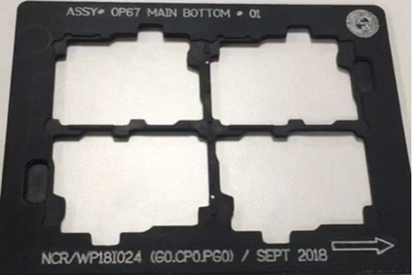
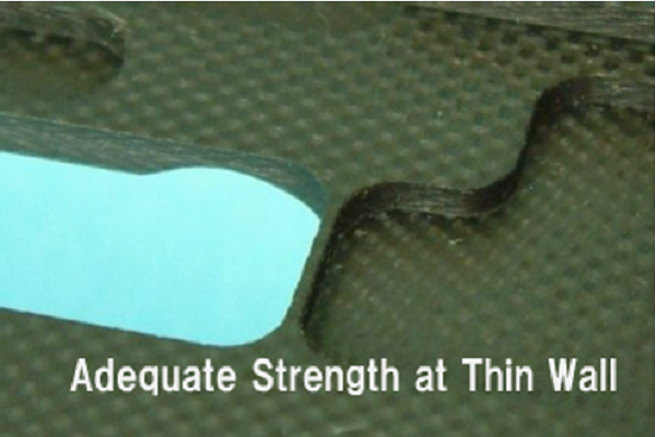
Laser cut stencils
High precision stencils made with the best raw material available globally . Smallest size of aperture that can be cut is 40micron. Our design expertise and German engineered precision machines ensure optimum solder paste for BGA’s, QFN’s , IC’s, 01005 and various other types of components. We follow IPC standards and calculate the area ratio and aspect ratio to decide the thickness and modification required for the apertures.
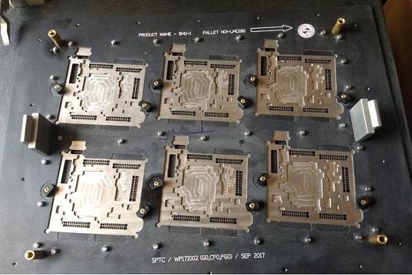
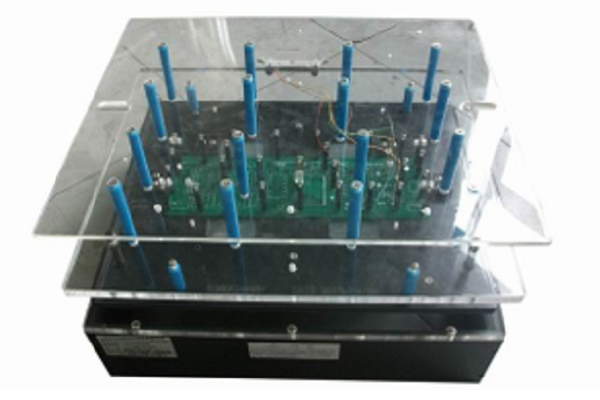
Multi Step Stencils
Some components require more or less solder paste compared to the other components on the same board. A stencil of multiple thickness needs to be used to give the optimum solder paste for each component. We use a special grade of SS , chemically etch the thickness and then laser cut the apertures.
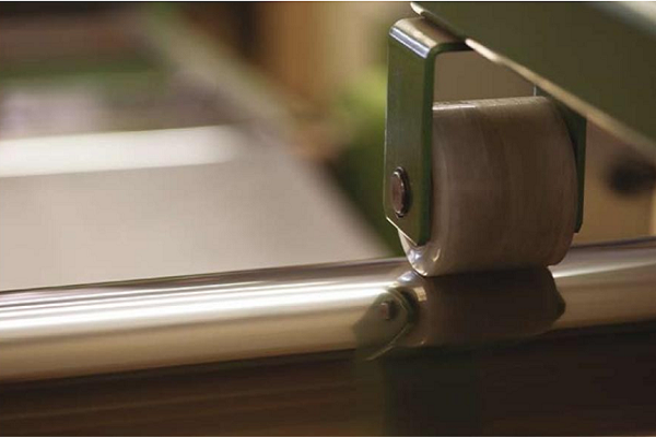
Nano Clear
Aculon’s latest nano coating technology to ensure smooth solder paste release and reduce the number of cleaning cycles. A two part wipes to be applied on the stencil which forms a nano coat within minutes. SPI machines accurately capture the improved solder paste release.
Stencil 2.0
A mechanical deburring process to remove micro burrs that occur during the laser cutting process. Improved solder paste release . Get the maximum transfer efficiency !
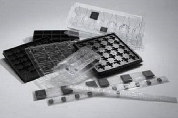
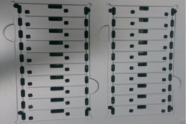
Micro stencil
Stencils without frames , used for prototype pcbs of small quantity where manual printing is done.
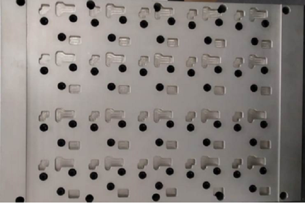
BGA reballing kit
Alpha Tetrabond Frame and Foil
Frameless foils.
Space saving upto 70%. Better tension than closest frameless competitor. Compatible with Dek Vector Guard.
Key attributes
Certificates
ISO 9001:2015
Reviews
Questions & answers
Ask the supplier — answers are visible to all buyers
No questions yet. Be the first to ask!
Know your supplier
VISION STENCILS PRIVATE LIMITED
Unverified<1 yr on BharatSealBangalore, Karnataka
Orders completed
—
On-time delivery
—
Reorder rate
—
Year founded
1992
Staff size
—
Certifications
1
%22%2F%3E%3Ctext%20x%3D%2250%25%22%20y%3D%2250%25%22%20dominant-baseline%3D%22central%22%20text-anchor%3D%22middle%22%20font-family%3D%22'DM%20Sans'%2Csystem-ui%2Csans-serif%22%20font-weight%3D%22800%22%20font-size%3D%22126%22%20fill%3D%22%231a1a1a%22%20fill-opacity%3D%220.14%22%20letter-spacing%3D%22-2%22%3EMS%3C%2Ftext%3E%3C%2Fsvg%3E)
%22%2F%3E%3Ctext%20x%3D%2250%25%22%20y%3D%2250%25%22%20dominant-baseline%3D%22central%22%20text-anchor%3D%22middle%22%20font-family%3D%22'DM%20Sans'%2Csystem-ui%2Csans-serif%22%20font-weight%3D%22800%22%20font-size%3D%22126%22%20fill%3D%22%231a1a1a%22%20fill-opacity%3D%220.14%22%20letter-spacing%3D%22-2%22%3ERS%3C%2Ftext%3E%3C%2Fsvg%3E)
%22%2F%3E%3Ctext%20x%3D%2250%25%22%20y%3D%2250%25%22%20dominant-baseline%3D%22central%22%20text-anchor%3D%22middle%22%20font-family%3D%22'DM%20Sans'%2Csystem-ui%2Csans-serif%22%20font-weight%3D%22800%22%20font-size%3D%22126%22%20fill%3D%22%231a1a1a%22%20fill-opacity%3D%220.14%22%20letter-spacing%3D%22-2%22%3EUP%3C%2Ftext%3E%3C%2Fsvg%3E)
%22%2F%3E%3Ctext%20x%3D%2250%25%22%20y%3D%2250%25%22%20dominant-baseline%3D%22central%22%20text-anchor%3D%22middle%22%20font-family%3D%22'DM%20Sans'%2Csystem-ui%2Csans-serif%22%20font-weight%3D%22800%22%20font-size%3D%22126%22%20fill%3D%22%231a1a1a%22%20fill-opacity%3D%220.14%22%20letter-spacing%3D%22-2%22%3ECJ%3C%2Ftext%3E%3C%2Fsvg%3E)